
Current events
Next talk on Tuesday in 3 days by Simone Sotgiu.
News 06.06.2025
New publication:Anisotropic supercurrent suppression and revivals in a graphene-based Josephson junction under in-plane magnetic fields
Site Content:
21.03.2025
New publication: Bluetooth sensors in phyphox with Arduino and MicroPython
A new publication by Staacks et al. about the Bluetooth interface of the physics education app "phyphox".
Abstract:
In order to extend the available sensors of smartphone experiments with cheap microcontroller-based external sensors, the smartphone experimentation app 'phyphox' has been extended with a generic Bluetooth Low Energy interface. Since its application requires an in-depth understanding of the underlying technologies, the direct use of that interface for educational purposes is limited. To avoid this difficulty, the functionality was encapsulated into an Arduino and MicroPython library. With these, also educators and learners with only rudimentary programming knowledge can integrate an app-based interface into microcontroller projects with only few lines of code. This opens a wide range of new learning opportunities, which are described exemplarily.
Published in Physics Education (preprint on arXiv)
25.02.2025
Timo Bißwanger successfully defended his PhD thesis
On Tuesday 25.02.2025, Timo Bißwanger successfully defended his PhD thesis. Congratulations to Dr. Timo Bißwanger on this fantastic accomplishment!
14.02.2025
New publication: Super-resolution imaging of nanoscale inhomogeneities in hBN-covered and encapsulated few-layer graphene
Adv. Sci. 18, 2409039 (2025) Encapsulating few-layer graphene (FLG) in hexagonal boron nitride (hBN) can cause nanoscale inhomogeneities in the FLG, including changes in stacking domains and topographic defects. Due to the diffraction limit, characterizing these inhomogeneities is challenging. Recently, the visualization of stacking domains in encapsulated four-layer graphene (4LG) has been demonstrated with phonon polariton (PhP)-assisted near-field imaging. However, the underlying coupling mechanism and ability to image subdiffractional-sized inhomogeneities remain unknown. Here, direct replicas and magnified images of subdiffractional-sized inhomogeneities in hBN-covered trilayer graphene (TLG) and encapsulated 4LG, enabled by the hyperlensing effect, are retrieved. This hyperlensing effect is mediated by hBN's hyperbolic PhP that couple to the FLG's plasmon polaritons. Using near-field microscopy, the coupling is identified by determining the polariton dispersion in hBN-covered TLG to be stacking-dependent. This work demonstrates super-resolution and magnified imaging of inhomogeneities, paving the way for the realization of homogeneous encapsulated FLG transport samples to study correlated physics.
12.02.2025
Contributing to the discussion of strategic directions of excellent teaching at RWTH
Christoph Stampfer had the opportunity to share more about our institute's experience with LLMs in physics teaching, especially with LandauAI (many thanks to Jan-Lucas Uslu) at the annual workshop of the "Studiendekan*innen" of RWTH Aachen University at Burg Obbendorf in Niederzier.
05.02.2025
Annual PGI-Forum fosters collaboration and innovation
Scientists from the Peter Grünberg Institute (PGI) gathered today for the annual PGI-Forum to share research updates, spark new collaborations, and exchange ideas. Christoph Stampfer's presentation on "2D Materials for Next Generation Computing" sparked engaging discussions. Once again, the forum proved to be a very lively event.
04.02.2025
Congratulations to Jan-Lucas Uslu on his admission to the PhD program at Stanford!
We warmly congratulate our former Bachelor’s and Master’s student, Jan-Lucas Uslu, on being admitted to the PhD program at the Department of Applied Physics at Stanford (California, USA). We a wish Jan-Lucas great success in his research and future endeavours!
21.12.2024
Season's Greetings from the 2D Materials and Quantum Devices Group
As the festive season approaches quickly, we at the 2D Materials and Quantum Devices Group would like to extend our warmest wishes to all for a Merry Christmas and a Happy New Year 2025!

16.12.2024
New publication: Benchmarking the integration of hexagonal boron nitride crystals and thin films into graphene-based van der Waals heterostructures
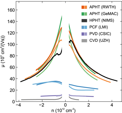
2D Materials 12, 015017 (2025) We present a benchmarking protocol that combines the characterization of boron nitride (BN) crystals and films with the evaluation of the electronic properties of graphene on these substrates. Our study includes hBN crystals grown under different conditions (atmospheric pressure high temperature, high pressure high temperature, pressure controlled furnace) and scalable BN films deposited by either chemical or physical vapor deposition (CVD or PVD). We explore the complete process from boron nitride growth, over its optical characterization by time-resolved cathodoluminescence (TRCL), to the optical and electronic characterization of graphene by Raman spectroscopy after encapsulation and Hall bar processing. Within our benchmarking protocol we achieve a homogeneous electronic performance within each Hall bar device through a fast and reproducible processing routine. We find that a free exciton lifetime of 1 ns measured on as-grown hBN crystals by TRCL is sufficient to achieve high graphene room temperature charge carrier mobilities of 80,000 cm2/(Vs) at a carrier density of |n| = 1012 cm-2, while respective exciton lifetimes around 100 ps yield mobilities up to 30,000 cm2/(Vs). For scalable PVD-grown BN films, we measure carrier mobilities exceeding 10,000 cm2/(Vs) which correlates with a graphene Raman 2D peak linewidth of 22 cm-1. Our work highlights the importance of the Raman 2D linewidth of graphene as a critical metric that effectively assesses the interface quality (i.e. surface roughness) to the BN substrate, which directly affects the charge carrier mobility of graphene. Graphene 2D linewidth analysis is suitable for all BN substrates and is particularly advantageous when TRCL or BN Raman spectroscopy cannot be applied to specific BN materials such as amorphous or thin films. This underlines the superior role of spatially-resolved spectroscopy in the evaluation of BN crystals and films for the use of high-mobility graphene devices.